Home > SMT Assembly News
In Figure 1, the solder has failed to wet the lead termination but has wetted the through hole. In this case, the plating was found to be an issue as the brass pins had not been correctly plated with copper before tin lead plating. The copper plating is necessary to stop zinc migration affecting the tin/lead surface. A minimum of 0.002µm is necessary for long solderable life with a minimum of 0.005µm of tin/lead over the copper. The components are clearly at fault and this is not a problem associated with the soldering process.
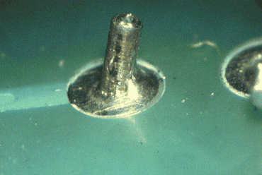
Figure 1: Here, the brass pins had not been plated with copper before tin lead plating.
In Figure 2, the solder failed to wet the surface of the lead during wave contact even though there is evidence of satisfactory wetting on the pad. This problem was caused by marginal solderability of the leads and the age of the 10% solids flux being used in production. Replacing the flux and changing it regularly after forty hours of operation solved the problem. Flux in an open tank degrades; its performance changes even if the solids content remains the same. Using components and making sure they are rotated in stores also reduces the issue reoccurring. Component suppliers generally only guarantee their parts are solderable for a period of twelve months.
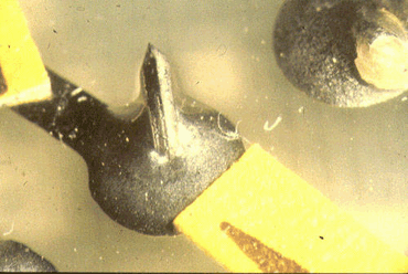
Figure 2: Degraded flux caused the solder to fail to wet the surface of this lead.
Poor solderability on tin/lead boards is uncommon if the correct thickness of tin/lead is applied to the pad surface. As a guide, a minimum thickness of 0.005µm should provide a solderable coating that will exceed a twelve month shelf life. It will most probably protect the surface in normal conditions for a couple of years and still be highly solderable.
In the case of the sample shown in Figure 3 the tin/lead was less than 0.002µm on the surface of the board. It was also a plated finish that had not been reflowed during board manufacture, hence the shorter shelf life of the product. Only part of the through hole pad surface has wetted with solder; the outer and inner edge of the pad has failed to wet.
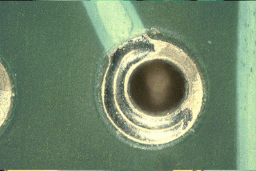
Figure 3: Only part of this through hole pad surface has wetted - the inner and outer edges have failed to wet.
The pad in Figure 4 has failed to wet during soldering and is undoubtedly caused by the poor solderability of the pad surface. The reason for the poor wetting of the pad is a little more difficult to define. The solderability of the board should be tested as the surface would appear to have dewetted just after soldering which is likely to be related to the PCB.
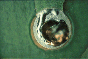
Figure 4: This defect was caused by the poor solderability of the pad surface.
Poor solderability of the pins can be caused by poor or thin plating or long storage times. Solderability of tin/lead pins normally is a function of the plating thickness or of the plating and the base materials. In the case of brass pins, the pin must first be plated with a 1-3µm layer of copper before the tin/lead is applied; otherwise zinc from the brass will affect the solderability very quickly.
Solderability is also related to thickness. If a coating of 0.005µm is present, it should provide in excess of one year's storage life. This coating thickness is relevant for any base materials. The example shown in Figure 5 is not a plating issue; it was caused by the printed board resin on the corner of the pins. If you look carefully you can see that only the corners of the pins has failed to wet. During pin insertion, the four corners of the pin have made an interference fit with the single-sided board, causing resin to smear along the corners.
When looking at any defects, don't jump to conclusions;, look at a number of defects using 10x magnification and just take a few minutes to think about the whole process, not just soldering.
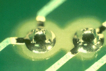
Figure 5: Only the corners of the pins here have failed to wet.
Figure 6 clearly shows poor wetting on the surface of the component leads with satisfactory pad wetting on the PCB. The component should be tested for solderability using a wetting balance or the dip and inspect test. Either the components have been stored for too long a period of time or the tin/lead coating on the leads was too thin. As an example, a tin/lead coating of 5µm should provide a solderable life in excess of one year.
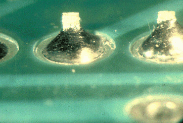
Figure 6: While the pad wetting is satisfactory, the component leads show poor wetting.
At first glance, the example in Figure 7 may be considered a skipped joint, but close examination shows it to be a solderability problem with the printed board coating. The gold surface coating is not wettable and needs to be discussed with the PCB manufacturer. It is normally caused by an out of balance electroless gold bath.

Figure 7: The gold surface coating here is not wettable.
Incomplete wetting or poor solder rise in a plated through hole will show up due to poor fluxing or pre-heat temperature. If both are satisfactory, it will be the surface coating of the board. The trend in the industry is to copper surface finishes, but care must be taken over their selection. Special assembly conditions should also apply to storage, washing boards, cure and reflow temperature.
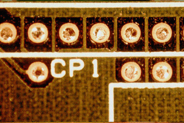
Figure 8: Incomplete wetting.
The solder joints on the IC in Figure 9 are satisfactory, with good fillets. The visual appearance of the leads are poor due to loss of the tin plating. Although the exposed leads will oxidise and are not likely to cause problems, the visual appearance will probably require the parts to be removed.
The loss of plating is due to poor initial plating probably during the preparation of the base lead frame prior to tin/lead coating. Loss of the coating is often seen at the lead to plastic interface due to mold flash contaminating the lead frame.
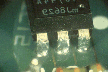
Figure 9: Poor initial plating caused this defect that is not likely to cause problems but will probably cause the part to have to be removed nonetheless.
Poor solderability of the pins is not acceptable as these would form unreliable joints. The brass pins in Figure 10 have failed to wet with solder, in fact the tin plating has separated from the base material during soldering. The brass pins should have been plated with 1-2µm copper before tin/lead plating. What was astonishing was the supplier of these parts said that the components were perfectly solderable!
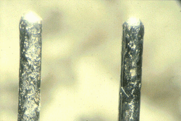
Figure 10: These brass pins should have been plated with 1-2µm copper.
The solderability of the pin in Figure 11 was poor--after solder immersion the lead has failed to wet. The reason for the problem was thin tin/lead coating that resulted in poor wetting. A coating of 5µm should be used as a minimum to give a 12 month shelf life. Generally solderability problems are less likely with high activity fluxes and may increase as companies move to low residue low activity materials.
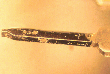
Figure 11: The lead failed to wet, thanks to a too-thin tin/lead coating.
Poor Penetration on a Printed Circuit Board
For a solder joint to form on the topside of a board, flux needs to be present in the plated through holes. The temperature of the topside of the board needs to have reached a minimum of 100-110°C. The most common process problem today with no clean is limited flux application. It is generally uncommon to have problems with through hole plating provided a board manufacturer's products are evaluated prior to use. It is also firmly uncommon to have contamination in the through hole causing this sort of problem. If flux penetration is present and correct pre-heat obtained then have the printed board tested.
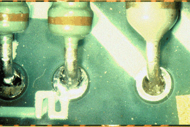
Figure 1: Poor penetration is caused by either inadequate flux application or inadequate pre-heating.
In Figure 2, the solder has failed to fill the plated through hole on one side of the component. The solder has wetted the PCB, but failed to fully wet the component lead, which is more likely to be flux related. If the fault is with the process conditions, there should be other positions on the board that have a similar problem. Simple solderability testing of the board and component termination should indicate if the fault is process or material related.
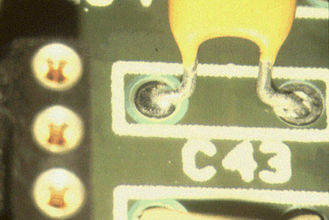
Figure 2: Poor penetration here is likely to be flux related.
Outgassing is still a common problem associated with wave and hand soldering. Basically when a board is soldered any moisture in the board close to the hole is heated and turned to vapor. If there is thin plating or voids in the plating, gassing can come through the plated hole wall. If solder is present in the hole, this will produce voids in the solder as it solidifies. The voids may appear as small holes in the surface of the joint, as shown in Figure 1, or much larger cavities.
Having the correct copper plating thickness in the through holes is the key. A minimum of 25µm of copper should be present on the surface of the hole walls.

Figure 1: Voids caused by outgassing.
Although a solder ball is present in Figure 1, it should have been referred to as a solder attachment rather than a ball. The solder has wet the track due to failure of the resist coating. The coating may have failed as it was applied over a tin/lead coating on the tracking or due to poor print thickness control. Care must be taken to ensure operators recognize the difference as any attempt to remove this type of ball manually will result in a damaged track.
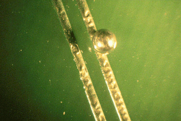
Figure 1: Manual removal of this solder attachment will damage the track.
Solder balling can be caused by poor process conditions with gassing from the flux during wave contact or excessive turbulence as the solder flows back into the bath which causes spitting. Solder balls can be ejected from the joint area during soldering due to excessive outgassing of the PCB. In Figure 2 shown a solder ball is attached to the base of the board on the edge of the resist and must have attached itself to the resist as it separated from the pin.
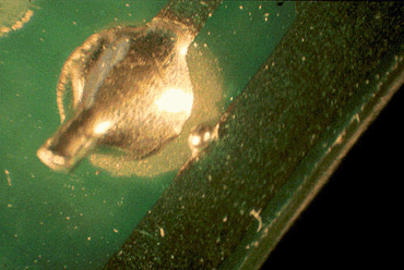
Figure 2: This solder ball must have attached itself to the resist as it separated from the pin.
In Figure 3, a solder ball is attached to the base of the board on the edge of the resist and must have attached itself to the resist as it separated from the pin.

Figure 3: Another solder ball attached to the edge of a resist.
Care should be taken with some solder balls. The example in Figure 4 is on a track and cannot be just knocked off. It is caused by squeeze out of the tin/lead from under the solder mask. or just simple adhesion. As the tin/lead becomes liquid during reflow or wave soldering, the tin/lead expands. The solder ball can form on a track. If the solder resist is thin, solder can wet during wave contact and leave a ball.
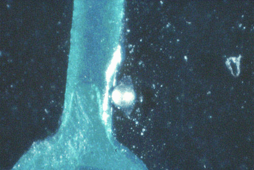
Figure 4: Solder on a resist can wet during wave contact and leave a ball.
Solder balling during wave soldering has always been around, but the elimination of cleaning after the soldering operation has made it more visible as a process problem. In the past, the solder balls were washed off the board surface during cleaning, out of sight out of mind!
Solder balls are caused by a number of process parameters. In Figure 5, the position of the balls is random. This type of defect is normally caused by spitting from the surface of the wave, which is associated with wave soldering parameters. If the solder is falling a distance from the printed board as the wave separates, the solder can literally splash back from the bath. If the preheat is incorrectly set or the quantity of flux applied increases, the evaporation of the solvent from the flux may be affected. Using a glass plate over the wave should show up the gassing problem. Ideally there should be minimal bubbles visible below the glass when it contacts the wave. The compatibility of the resist and flux should be examined; often the mask can contribute to solder ball adhesion.

Figure 5: Solder balls on this board were caused by spitting from the surface of the wave.
The causes of solder balls are numerous, and they have always been present on the bottom side of printed boards. It has been the increase of the use of no clean low residue soldering that has focused more attention on the problem.
Regardless of the cause, if the solder balls do not adhere to the solder mask when leaving the solder wave, the problem is mostly eliminated. Selecting the best solder mask is the best solution to making a board design robust.
Solder balls are caused by gassing and spitting of the flux on the surface of the wave or by solder literally bouncing back from the solder wave. This is caused by excessive back flow in air or too high a drop in nitrogen environments.
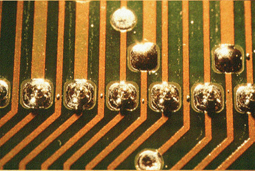
Figure 6: More solder balls caused by spitting.
In Figure 7, the solder balling is random and more likely the result of solder balls spitting or bouncing up from the solder wave. This is caused by volatile materials still remaining from the flux or the height of the wave separation. Try using a piece of white card placed over the wave. Leave it there with the wave running but without boards being processed. Then try the same test with boards going through the machine. This will pinpoint the cause of the problem.
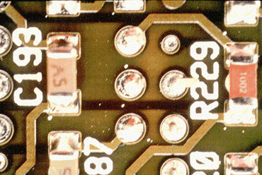
Figure 7: More solder balling caused by spitting. Place a white card over the wave to pinpoint the cause of the problem.
Solder flags or spikes are due either to inconsistent flux application or poor control of solder drainage from the wave.
If poor flux application is the cause, there will be other evidence on the surface of the board, like thin whiskers of solder similar to snail trails on a garden path.
Poor control of separation from the solder wave would tends to be a random fault, not on the same contacts every time. This is due to the back flow of the wave not being set correctly on a lambda style wave. The solder should flow at the same speed and direction as the board during separation from the wave. Running slightly faster will not normally cause spiking, but running slow or not flowing at all will increase spikes.
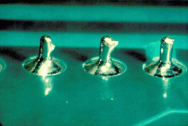
Figure 1: Solder flags or spikes.
If the spikes are always on the tip of the leads it may be a solderability issue caused by bare cut ends. If leads are cut by the supplier or cut and stored for a long period of time, the bare end of the lead will oxidise and be difficult to wet with solder. If the lead is slow to wet, it will also be slow to drain, hence a spike can form.
On some occasions, the spiking can be a thermal problem simply eliminated by a longer immersion time in the wave or increase pre heat. A component that has a high mass may have a lead of the same size as other parts. During pre-heat of the board there may not be an opportunity for heat to be absorbed by the lead to overcome this thermal load. As the leads of the component separate from the wave they will cool much more quickly, leaving either spikes or shorts.
The solder flags shown in Figure 2 are probably due to inconsistent fluxing, which should be visible on other areas of the board. The length of the pins is also excessive. Lead length should not exceed 1.5-2.0mm below the level of the board. Shorting can also occur during exit from the back of the wave if the component leads are dragged through the wave oxide layer rather the exiting from a clean surface.
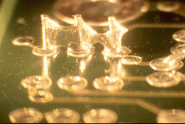
Figure 2: Inconsistent fluxing likely caused these solder flags.
Solder shorts are generally on the increase in the wave soldering process. This is due to the ever decreasing component pitches used in manufacture. In the past, the pitch of terminations were 0.050". Now we see many conventional terminations being used on a 0.025" pitch.
Solder shorting occurs when the solder does not separate from two or more leads before the solder solidifies. Increasing the flux solids or quantity is one way of decreasing shorting. A reduction of the lead length and the pad size will reduce the amount of solder being held on the base of the board. Figure 1 shows a connector on a 0.025" pitch that was improved through changes in the pad design. Alternative pads were increased in length on the exit side of the wave. This made the actual separation distance between the adjacent termination larger and decreased the shorting.
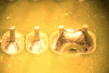
Figure 1: A solder short on a connector with a 0.025" pitch.
A solder short on the top side of a printed board is unusual, but it can occur. In Figure 2, the solder shorts were seen on IC leads on a single sided printed board. During contact with the wave, the pressure was so high that shorts occurred due to excessive solder penetration. This type of defect is more likely to be seen on any of the vibrating waves produced by three companies to aid surface mount assembly. It would be more likely to occur on single-sided board as the hole-size-to-lead ratio is often larger, due to the tolerances on these cheaper laminates.
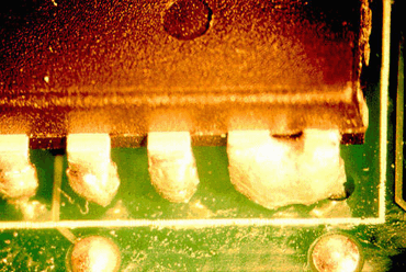
Figure 2: A rare solder short on the top side of a printed board.
Solder shorts are becoming a major problem in wave soldering, particularly as component pitches continue to decrease. In Figure 3, shorts are seen on a pin grid array (PGA) device. Due to the close proximity and the number of pins, the solder separation is impeded from the base of the board. Shorting can occur due to poor fluxing, incorrect pre heat or wave separation. All shorting can be decreased through good design rules, with reductions in pad size and component lead length. In the case of the example shown in Figure 3, it was necessary to change the solids content of the flux while still retaining a no clean process. Using a hot air knife failed to improve the process due to the high mix of boards and pin lengths.

Figure 3: Shorts on a pin grid array.
As boards become more heavily populated, shorting becomes more of a problem. A hot air knife after the solder wave can eliminate some problems, but most can only be fixed by good design. Increasing the flux solids will improve the drainage on all joints. In Figure 4, the pin length is correct at 1-1.5mm, but the surface pads could be reduced in size. With smaller pads, less solder is retained on the board to short between pins. If this is the only defect area on the board, then a nice fixit is a glue dot placed between the two pins by your placement department.
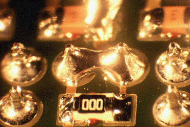
Figure 4: Smaller pads would have decreased the likelihood of this short occurring.
SOIC devices should be the limit for underside mounted components. Decreasing the pitch below 0.050" pitch will always increase defect levels or increase engineering time coaxing the process to solder 0.025" parts. Solder shorts are common on SOIC devices. If the short is in the middle of the row and the pad width is below 0.022", it is a process problem. Fluxing is the first area to examine, then look at adjustment to the contact time in the wave. Often changing the angle of the conveyor eliminates this defect. Unfortunately many wave soldering systems do not now allow this adjustment.
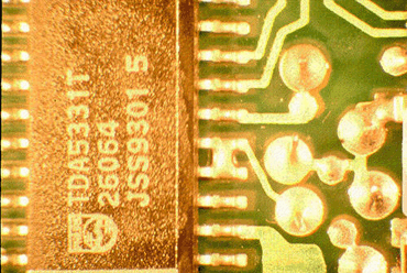
Figure 5: Solder shorts are common on SOIC devices.
Wave soldering devices below 0.050" pitch should be avoided and questioned during design for manufacture (DFM) reviews of new designs. Yes, it can be done, but it takes a lot more effort from machine and process engineers. Soldering 0.032" pitch can be achieved, 0.025" is problematic and using 0.020" on the base of the board requires more rework staff.
The shorting example in Figure 6 is seen at the top of the pins on a QFP device and may be improved by increasing the solid of the flux. This defect is often caused by incorrect pre-heat or limited time in the wave. The thermal effect of the device can tend to cool the solder, slowing drainage. On some occasions when the shorts are at the top of the lead form, it is a solderability issue. If a lead area close to the plastic body is slow to wet, it is also slow to drain, hence a short. As with SOIC devices, QFPs benefit from solder thiefs on the trailing edge of the parts, but only if the solder shorts are always on the last two pins. The solder thief pad should always be a minimum of three times the length of the last pad and on the same pitch. With QFPs, the device is also positioned at 45° to the direction of travel through the wave. Try gluing some components to the base of a glass plate; this will help you convince both engineers and design engineers that design for manufacture is a must.
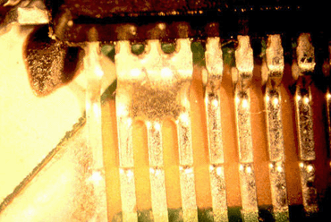
Figure 6: Shorting at the top of the pins on a QFP.
Solder shorts can result from poor solderability of the pins. In Figure 7, there are solder spikes on the ends of the leads due to the poor solderability of the bare tips of the leads. If a termination is slow to wet it is generally slow to drain hence increasing the incidence of solder shorting.
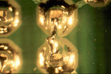
Figure 7: Poor solderability of bare tips caused these solder spikes and subsequent short.
Unsoldered surface mount joints are referred to as solder skips where the termination does not have any solder. It is caused by incorrect chip wave height or gassing of the flux on the underside of the board.
As Figure 1 shows, the resist thickness can also cause the problem or make it worse. Solder resist or mask should be level with the pad surface or below it for the ideal assembly conditions. If the mask is thick it creates a cavity around the pad where flux vapours are trapped forming a bubble. The solder cannot displace the vapour easily to form a joint.
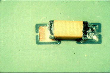
Figure 1: Resist thickness contributed to this solder skip.
While any surface mount solder joint not wetted with solder is generally referred to as a solder skip, some people refer to these as insufficient solder joints, which is misleading.
During assessment of the problem, it is important to check if a fresh coating of solder is on the pad or on the component termination. Often, the presence or lack of a new solder coating on the leads can indicate the root cause of the problem.
The most common causes of skipping are incorrect chip wave height, gassing of flux under the board surface or excess resist thickness. Each of these faults can be easily fixed, although the resist may take a little longer if you have a large stock of boards, but review your PCB specification.
In Figure 2, adhesive has contaminated the pad surface. Although no adhesive deposit is visible, some adhesives allow an invisible film to bleed out from the dot area during curing. Try evaluating your adhesive.
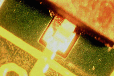
Figure 2: Adhesive contamination on the pad surface caused this solder skip.
The example in Figure 3 is clearly not soldered, and the waves could not have been that badly adjusted in a professional company, could they? It is more likely that the board was not correctly positioned in the finger conveyor or in the pallet. The pallets may be distorted or the clips are not holding the board flat.
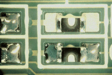
Figure 3: It is likely that the board was not correctly positioned on the finger conveyor or in the pallet.
Sunken joints on the base of the board are most commonly caused by outgassing from the printed board. Like small voics in the solder fillets (referred to as pin holes or blow holes), they are seen as another process indicator. If the copper plating thickness remains a minimum of 25µm in the barrel of the hole, moisture will not outgass through the copper during soldering.
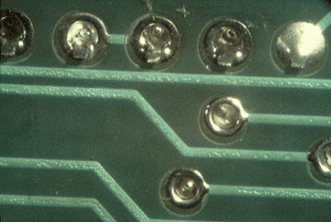
Figure 1: Sunken solder joints caused by outgassing.
In Figure 2, the insulation on the body of the part was also found on the top of the leads, which made joint formation difficult to achieve.
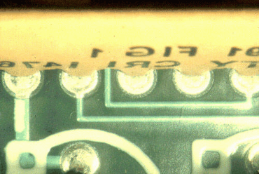
Figure 2: The component's insulation interfered with joint formation.
The most common cause of sunken joints is the hole-to-lead ratio. If the hole is large in comparison to the lead diameter, the solder literally drops in or out of the hole.
In cases where the solder has not reflowed directly on the top side of the board, sunken joints on the tops side of the board can be caused by incorrect pre-heat or poor fluxing. This would not be the case in the example shown in Figure 3 as the tin/lead has either reflowed on to the top side or caused the existing solder coating to reflow.
Sunken joints on the base of the board may be caused by outgassing. If the soldering process is functioning correctly when the hole outgasses the solder tends to shrink back into the hole to fill the void.
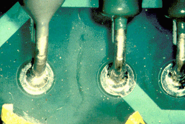
Figure 3: Adhesive contamination on the pad surface caused this solder skip.
Normally this is a cosmetic issue but should be investigated for the real cause. When running a thicker board it is probable that the soldering process or dwell times may have changed.
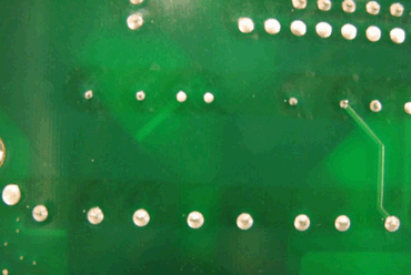
Figure 1: Dark stripes on the solder mask after selective soldering.
There is no reference to the board finish, solder alloy being used or flux type - water or alcohol based. These are important when conducting analysis of the process problem.




Contact: Mr Tommy
Phone: +86 13691605420
Tel: +86 -755-85225569
Email: tommy@flason-smt.com
Add: 94#,Guangtian Road,Songgang Street,Bao an District Shenzhen China